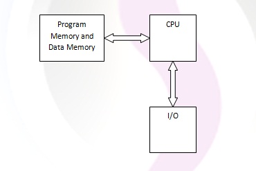
Wednesday, November 2, 2016

8051 HARDWARE ARCHITECTURE

8051 HARDWARE ARCHITECTURE


Introduction
The 8051 is an 8-bit, low-power, high-performance microcontroller. There are a large number of devices in the 8051 family with similar architecture and each member of the family is downward compatible with each other. The basic 8051microcontroller has the following features:
  •     4 Kbytes of program memory
  •       256*8 RAM data memory
  •       32 programmable I/O lines
  •       Two 16-bit timer/counters
  •       Six interrupt sources
  •       Programmable serial UART port
  •       External memory interface
  •     Standard 40-pin package

Various Features of 8051 Microcontroller

Various Features of 8051 microcontroller are given as follows

  • 8-bit CPU
  • 16-bit Program Counter
  • 8-bit Processor Status Word (PSW)
  • 8-bit Stack Pointer
  • Internal RAM of 128bytes
  • Special Function Registers (SFRs) of 128 bytes
  • 32 I/O pins arranged as four 8-bit ports (P0 - P3)
  • Two 16-bit timer/counters : T0 and T1
  • Two external and three internal vectored interrupts

Pin out Description

Pins 1-8: Port 1 Each of these pins can be configured as an input or an output.
Pin 9: RS A logic one on this pin disables the microcontroller and clears the contents of most registers. In other words, the positive voltage on this pin resets the microcontroller. By applying logic zero to this pin, the program starts execution from the beginning.
Pins10-17: Port 3 Similar to port 1, each of these pins can serve as general input or output. Besides, all of them have alternative functions.
Pin 10: RXD Serial asynchronous communication input or Serial synchronous communication output.
Pin 11: TXD Serial asynchronous communication output or Serial synchronous communication clock output.
Pin 12: INT0 Interrupt 0 input.
Pin 13: INT1 Interrupt 1 input.
Pin 14: T0 Counter 0 clock input.
Pin 15: T1 Counter 1 clock input.
Pin 16: WR Write to external (additional) RAM.
Pin 17: RD Read from external RAM.

Pin 18, 19: X2, X1 Internal oscillator input and output. A quartz crystal which specifies operating frequency is usually connected to these pins. Instead of it, miniature ceramics resonators can also be used for frequency stability. Later versions of microcontrollers operate at a frequency of 0 Hz up to over 50 Hz.
Pin 20: GND Ground.

Pin 21-28: Port 2 If there is no intention to use external memory then these port pins are configured as general inputs/outputs. In case external memory is used, the higher address byte, i.e. addresses A8-A15 will appear on this port. Even though memory with capacity of 64Kb is not used, which means that not all eight port bits are used for its addressing, the rest of them are not available as inputs/outputs.
Pin 29: PSEN If external ROM is used for storing program then a logic zero (0) appears on it every time the microcontroller reads a byte from memory.
Pin 30: ALE Prior to reading from external memory, the microcontroller puts the lower address byte (A0-A7) on P0 and activates the ALE output. After receiving signal from the ALE pin, the external register (usually 74HCT373 or 74HCT375 add-on chip) memorizes the state of P0 and uses it as a memory chip address. Immediately after that, the ALU pin is returned its previous logic state and P0 is now used as a Data Bus. As seen, port data multiplexing is performed by means of only one additional (and cheap) integrated circuit. In other words, this port is used for both data and address transmission.
Pin 31: EA By applying logic zero to this pin, P2 and P3 are used for data and address transmission with no regard to whether there is internal memory or not. It means that even there is a program written to the microcontroller, it will not be executed. Instead, the program written to external ROM will be executed. By applying logic one to the EA pin, the microcontroller will use both memories, first internal then external (if exists).
Pin 32-39: Port 0 Similar to P2, if external memory is not used, these pins can be used as general inputs/outputs. Otherwise, P0 is configured as address output (A0-A7) when the ALE pin is driven high (1) or as data output (Data Bus) when the ALE pin is driven low (0).
Pin 40: VCC +5V power supply.


Tuesday, November 1, 2016

HOW TO GET UNLIMITED GEMS IN CLASH OF CLANS

IT IS VERY SIMPLE ALL CAN TRY


Having more than 100 million downloads on iOS and Android, Clash of Clans is definitely a well-liked and well received game. Quickly after the December upgrade, some Clash of Clans gamers experienced several impediments. Thus, a brand new update will roll out and the loot system will be enhanced. But, that part is not the only enhancement, so let’s have a look-see at the new 2016 changes that will roll out with the Clash of Clans update.

Star Bonus
Supercell clearly stated that new improvements are on the way. Star Bonus is one of them and it will be given to those of you who play Clash of Clans on a daily basis. So, when you complete the daily goals, you’ll be rewarded with resources.

Treasury
The Treasury is something new that will be stored in the Clan Castle. Now, gamers can store their most treasured resources such as the Loot Cart, the Star Bonus even and a lot more. If you’re attacked by enemies, you’ll lose only a small percentage of the treasury.


Loot Cart
Every base will now have a Loot Cart. This is your prize for having a solid defense, so after you are attacked you can get your money back. Here is how it will go down: if an enemy robs you of 300K from the village, the loot cart will give you almost 25% of your money back. So, this will bring good things for the economy of the game
.


Wednesday, October 26, 2016

MICROCONTROLLER ARCHITECTURE

MICROCONTROLLER ARCHITECTURE
                
                   There are two types of MICROCONTROLLER architectures. They are
                                      1. von Neumann
                                       2. Harvard


          1. Von Neumann Architecture

                             The von Neumann architecture allows for one instruction to be read from memory or data to be read/written from/to memory at a time. In other words, an instruction fetch and data operation cannot be performed at the same time. Instructions and data are stored in the same memory subsystem and share a communication pathway or bus to the CPU.


        2. Harvard Architecture

                                       The Harvard architecture alternatively consists of separate pathways or buses for interaction between the CPU and memory. The separation allows for instructions and data to be accessed concurrently. Also, a new instruction may be fetched from memory at the same time another one is finishing execution, allowing for a primitive form of pipelining. Pipelining decreases the execution time of one instruction, but main memory access time, in many cases, is a major bottleneck in the overall performance of the system. 


Tuesday, October 25, 2016

PERIPHERALS AND ADVANTAGES OF EMBEDDED SYSTEM

PERIPHERALS USED WITH EMBEDDED SYSTEM

Embedded Systems communicate with the outside world via peripherals such as:
  •   Serial Communication Interfaces (SCI): RS 232, RS 422, RS 485 etc.
  •   Synchronous Serial Communication Interface: I2C, SPI, SSC and ESSI (Enhanced Synchronous Serial Interface)
  •   Universal Serial Bus (USB)
  •   Multi Media Cards (SD Cards, Compact Flash etc.)
  •   Networks: Ethernet, Lon Works etc.
  •   Field Bus: CAN Bus, LIN Bus PROFIBUS etc.
  •   Timers: PLL (s), Capture/Compare and Time Processing Units
  •   Discrete IO: aka General Purpose Input/output (GPIO)
  •  Analog to Digital/Digital to Analog (ADC/DAC)
  •   Debugging: JTAG, ISP, ICSP, BDM Port, BITP, and DP9 ports.


       ADVANTAGES OF EMBEDDED SYSTEM
              
  •        Design and Efficiency
  •         Cost
  •         Accessibility
  •         Maintenance


COMPONENTS OF AN EMBEDDED SYSTEM

COMPONENTS OF AN EMBEDDED SYSTEM
                       
                              There are two parts in an embedded system. They are

                                                1. HARDWARE PART
                                                2. SOFTWARE PART


 1. HARDWARE PART

                              This hardware part contains controllers, sensors, power supplies, and output devices.


2. SOFTWARE PART
   
                              This is the coding part. In this part we can write the source code to make the conrtollers work. It can be written any languages namely c,c++,python,and so.


EMBEDDED SYSTEM

DEFINITION OF AN EMBEDDED SYSTEM

                  An embedded system is a computer system designed for specific control functions within a larger system, often with real-time computing constraints. It is embedded as part of a complete device often including hardware and mechanical parts. By contrast, a general-purpose computer, such as a personal computer (PC), is designed to be flexible and to meet a wide range of end-user needs.


Evolution of Embedded System

                         The Minute-man I & II missiles are intercontinental ballistic nu-clear warheads, produced by Boeing in the 1960’s.Due to the large quantities of ICs used in the guidance system of Minuteman II missiles, prices for ICs fell from 1000$ each to 3$ each. This lead to wide adoption of embedded systems in consumer-electronics in the 1980’s.

                      Nowadays embedded systems can be found in devices from digital watches to trac control systems. The broad range of applications with totally different requirements leads to various implementation approaches. The range of hardware used in embedded systems reaches from FPGAs to full blown desktop CPUs which are accompanied by special-purpose ICs such as DSPs.